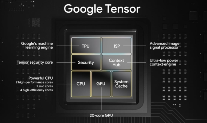
Since their launch, Google Tensor chipsets have relied on Exynos chips manufactured by Samsung. However, this is set to change with the upcoming Tensor G5, as Google plans to transition to TSMC’s process node for production. Android Authority has published a detailed report from Google’s gChips division, shedding light on what we can expect from the Tensor G5 and G6 SoCs.
Google’s Tensor G5, codenamed “Laguna,” powers the upcoming Pixel 10 series and uses TSMC’s 3nm-class N3E process. This matches the process node in Apple’s A18 Pro chip for the iPhone 16 Pro series, positioning it as one of the top manufacturing technologies available today.

In terms of performance, the Tensor G5 will feature a revamped CPU cluster with 1 Arm Cortex-X4 prime core, 5 Cortex-A725 performance cores, and 2 Cortex-A520 efficiency units. The GPU is also getting an upgrade to a dual-core Imagination Technologies (IMG) DXT-48-1536 unit, clocked at 1.1 GHz.
This new GPU will introduce ray tracing capabilities, a first for Tensor chipsets, and will provide GPU virtualization for enhanced graphics performance in virtual machines. Additionally, Google is promising a 14% boost in AI performance thanks to a new NPU.
Looking ahead, Google plans to use TSMC’s upcoming N3P node for the Tensor G6, codenamed “Malibu.” Though still a 3nm process, N3P promises significant improvements in performance, power efficiency, and size. According to leaked documents, it will offer a 5% increase in frequency compared to N3E, consume 7% less power, and take up 4% less surface area.


